Theory of Operation of Logarithmic Amplification
Theory of Operation of Logarithmic Amplification
In this technical note, we discuss some general principles relating to logarithmic amplification. First of all, no amplifier can produce a logarithmic transfer function over a dynamic range which includes an input signal level of zero, since log 0 = -∞. All logarithmic amplifiers must therefore specify a signal range over which they will "log". The classic log amp discussed in most introductory texts exploits the I-V characteristics of a diode junction, and consists of a diode feedback on an inverting operational amplifier. This approach works well (over a dynamic range of >4 decades) at low speeds (less than 1 MHz), if the circuit is properly temperature-compensated. At higher speeds the performance is woeful, and other schemes⁽¹⁾ to approximate a logarithmic transfer are used.
The basic idea of the most common approach can be understood by examining the circuit shown in Fig. A1, below.


For M = N-1 and M = N the approximation starts to fail, and corrective measures such as "linear extension" are needed. In the case of DLVAs, such measures are needed in any case, because of detector roll-off.

The cusps shown in the transfer curve of Fig. A2 result from the assumption that the amplifiers are hard limiting. In a real circuit, the effect of the cusps can be made to be minimal.
There is one serious problem with a circuit like the one described: the minimum input voltage required to limit a single stage silicon transistor is about 100 mV at room temperature, and that is when the amplifier is not fed back in any manner. Thus the start of logging would be at about 20 mV input for the above circuit, which means that to get a 4 decade dynamic range, input signals would have to go as high as 200 volts!
This problem can be circumvented by using a circuit architecture like the one shown below in Fig. A3.

A1 and A2 are linear amps, and remain linear up to a voltage which is sufficient to limit the log stages L1 ... L4 (about 500 mV).
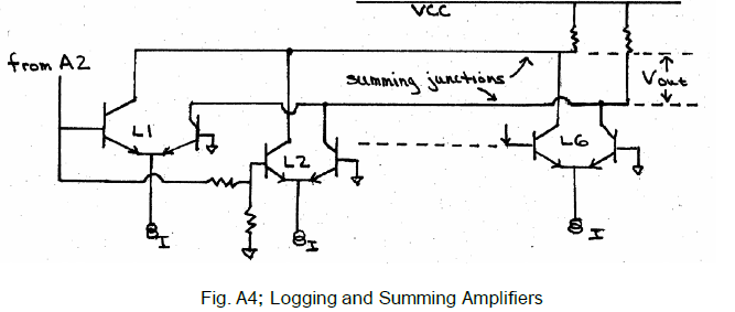
The log stages are simply undegenerated diff pairs, as shown in Fig. A4, which are not hard-limiting. This smooths the cusps of the transfer curve sketched in Fig. A2. The "summing amp" is simply two resistors.